

As Artificial Intelligence (AI) workloads continue to grow in complexity, memory architectures must evolve to handle the immense data processing demands of machine learning, deep learning and real-time analytics. Conventional memory hierarchies are increasingly bottlenecked by bandwidth limitations, latency issues and energy inefficiencies, making multi-layered memory architectures a necessity for next-generation AI applications. Erik Hosler, an authority on AI-driven innovation in semiconductor engineering, recognizes the critical role of memory innovation in sustaining AI performance, ensuring that hardware can keep pace with the exponential growth in computational demands.
Why AI Needs Multi-Layered Memory Architectures
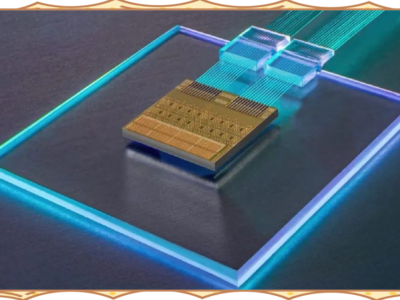
AI workloads generate and process vast amounts of data, requiring high-speed access to memory with minimal latency. Traditional DRAM-based architectures struggle to meet these demands, as data transfer rates are often constrained by limited bandwidth and inefficient memory hierarchies. Multi-layered memory architectures provide a solution by integrating High-Bandwidth Memory (HBM), 3D NAND and next-generation persistent memory into a cohesive, tiered storage system.
By stacking multiple memory layers vertically, these architectures enable faster data retrieval, reduced energy consumption and improved scalability, which are crucial for AI-driven applications such as natural language processing, computer vision and autonomous systems. Tighter integration between memory and processing units ensures higher throughput, allowing AI models to train and infer more efficiently.
Overcoming Memory Bottlenecks in AI Computing
One of the biggest challenges in AI computing is overcoming the memory wall, where the speed of data movement between processors and memory becomes a limiting factor. Multi-layered memory architectures address this issue by incorporating:
High-Bandwidth Memory (HBM) – Utilizing vertically stacked memory layers with wide data buses to maximize bandwidth.
Hybrid Memory Solutions – Combining DRAM, Non-Volatile Memory (NVM) and Storage-Class Memory (SCM) for efficient data access.
Near-Memory and In-Memory Computing – Reducing data transfer distances by placing computational tasks closer to memory layers.
Advancements in Lithography for Multi-Layered Memory Scaling
As memory architectures scale beyond hundreds of layers, precision in fabrication becomes critical. Erik Hosler remarks, “Innovation in light source development and lithography is shaping the future of semiconductor applications.” His insight underscores the role of EUV lithography and high-precision stacking techniques in ensuring efficient, defect-free multi-layered memory production.
The Future of AI-Optimized Memory Architectures
As AI continues to drive innovation in computing, memory architectures must evolve to sustain higher processing capabilities. Future developments in multi-layered memory will focus on:
Dynamic AI Memory Management – Optimizing memory allocation based on AI workload patterns.
3D Stacked MRAM and ReRAM – Providing high-speed, non-volatile storage solutions for edge AI.
Photonics-Integrated Memory – Leveraging optical interconnects for ultra-fast data transfer.
Multi-layered memory architectures will reshape AI computing by pushing the boundaries of scalability, efficiency and performance, ensuring real-time processing capabilities for future AI-driven technologies.


Comments